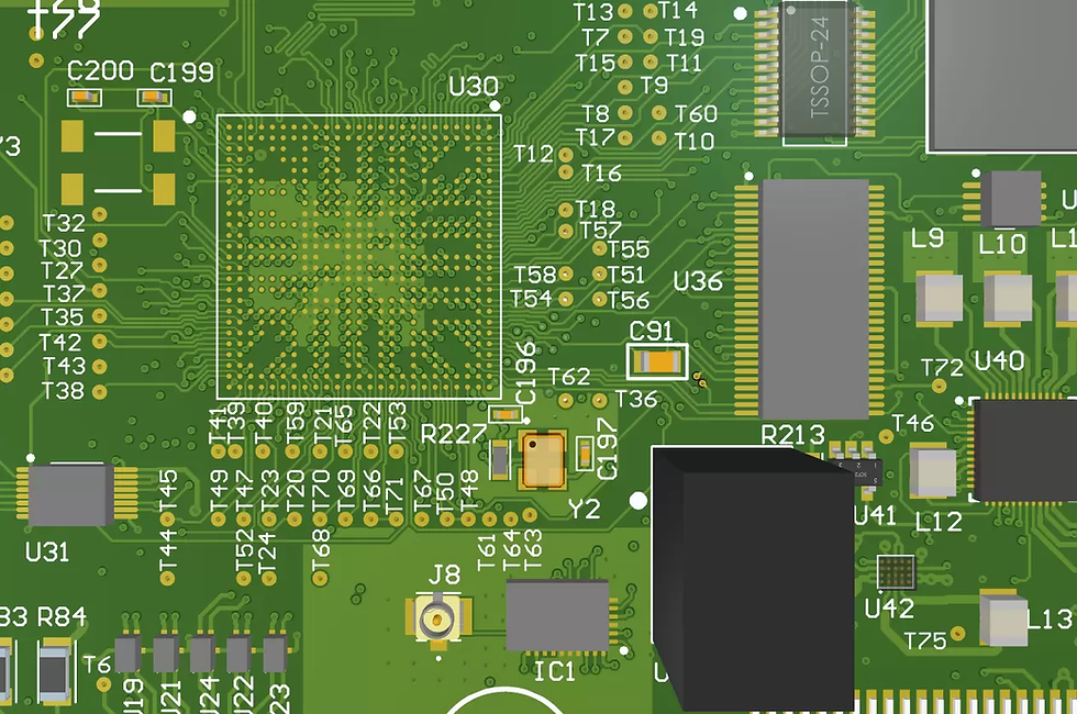
PCB Design Rule Check
- Sep 11, 2023
- 4 min read
Electronic manufacturing is a complex process, and at the heart of it lies circuit design. Yet, designing electronic circuits can be incredibly challenging due to the intricate nature of electronic components, and even seasoned professionals are not immune to making errors. Therefore, ensuring error-free manufacturing processes is paramount, and one effective method to achieve this is through PCB Design Rule Checking (DRC).

Understanding PCB Design Rule Checking:
PCB Design Rule Checking, or DRC for short, is a critical process that involves scrutinizing a set of guidelines established by designers to validate whether the schematic and layout of a circuit board adhere to manufacturing requirements. By conducting DRC inspections, designers can ensure that their designs consider various critical factors, detect errors early in the design phase, and make timely corrections.
PCB design rule checking is instrumental in identifying discrepancies and issues that may arise during the manufacturing process. These issues can encompass aspects such as circuit wiring and line width. Typically, designers utilize specialized software to craft the board's layout. Each manufacturing facility adheres to a set of predefined rules, encompassing parameters like minimum via size and line spacing.
When Does Design Rule Checking Occur?
Design rule checking is a pivotal phase valued by professional manufacturers. Once the design files are in the hands of the manufacturer, they initiate the PCB design rule check promptly. This inspection process serves as a litmus test to verify whether the submitted design aligns with the manufacturer's stipulated standards. Any discrepancies unearthed by the DRC are swiftly identified, and appropriate warnings are issued. Subsequently, the manufacturer communicates these issues to the designers, highlighting areas that require adjustments or modifications within the layout.
It's important to note that the specific requirements for PCB design rule checking can vary from one manufacturer to another. Hence, PCB designers should conduct their own meticulous DRC checks before submitting their designs to manufacturers, ensuring strict compliance.
PCB Design Guidelines Checklist
Vertical Routing Guidelines:
These guidelines are employed to optimize the arrangement of signal traces when transitioning from one layer to another, especially in densely packed circuit layouts. The primary goals are to minimize the risk of pattern radiation and ensure seamless signal transition between different layers.
Additionally, this rule can help ensure the correct placement of stitched vias or capacitors, particularly in areas connected to the network.
Crosstalk Mitigation Guidelines:
Crosstalk, which can lead to operational glitches, is a critical concern in PCB design. These guidelines identify areas where unwanted crosstalk may occur in sensitive circuit networks.
Detecting crosstalk issues manually can be challenging, making these guidelines a valuable tool in mitigating interference.
Filter Positioning Guidelines:
These guidelines focus on the placement of filters in proximity to connector pins. Proper filter placement helps minimize potential noise interference on the connector pins.
Correct filter positioning is vital for reducing electromagnetic interference (EMI) risks and safeguarding sensitive signals from disruption. Improper placement can lead to EMI failures.
Decoupling Capacitor Placement Guidelines:
Meeting the decoupling capacitor requirements of each component is a critical aspect of PCB design. However, manually verifying the positioning of these capacitors can be time-consuming and prone to errors.
Decoupling capacitor placement guidelines efficiently identify any misaligned decoupling capacitors, enhancing design reliability.
Signal Power Supply Guidelines:
These guidelines are vital for detecting discontinuities between the power planes of integrated components and the reference planes connecting traces. Violating this guideline can result in EMI-related malfunctions and radiation issues.
Accurate planning of signal power supply is essential to ensure circuit stability and prevent unnecessary interference.
Ground/Power Trace Width Guidelines:
Ensuring adequate trace width for ground and power traces is crucial. These guidelines detect traces that are inadequately wide, which can lead to issues like inadequate current flow, excessive heat generation, and insufficient power delivery to components.
Proper trace width planning is pivotal for maintaining circuit stability and optimal performance.
Verifying Differential Symmetry with Design Rule Checking
In the realm of PCB designs, it's a common practice to incorporate multiple differential pairs, including those with 100-ohm and 50-ohm differential impedances. These differential pairs are typically defined separately within the layout tool's constraint manager, and the PCB tool seamlessly generates distinct constraint classes for them. This level of integration empowers designers to efficiently manage diverse rules for the two differential nets.
To attain optimal functionality, meticulous design of differential impedance traces is essential. Factors such as trace placement, spacing, and length symmetry significantly impact performance. Consequently, the differential pair rule becomes invaluable in evaluating the consistency of these attributes.
PCB designers can tailor rule parameters, such as maximum and minimum allowable trace lengths, to meet specific requirements. Given that each differential trace comes with unique impedance specifications, PCB DRC tools can dynamically adjust various design parameters based on these rule parameters.
Here is a selection of online DRC PCB tools:
Advanced Designer (Altium Designer): Altium Designer stands out as a robust tool equipped with comprehensive PCB design rule checking capabilities. It offers a plethora of options for scrutinizing the integrity of your PCB design and is held in high regard among professionals.
Simple EDA (EasyEDA): EasyEDA features a DRC function that adeptly identifies a range of errors. Not only is this online tool compatible with multiple operating systems (macOS, Windows, Linux), but it also boasts a rich component library and cloud-based collaboration, facilitating seamless teamwork on projects.
KiCad EDA: KiCad EDA is a dependable PCB design tool that aids in crafting top-tier circuit boards. It spans various operating systems (macOS, Windows, Linux) and provides all the necessary files, along with user-friendly online tools.
In Conclusion
Throughout the PCB design process, while DRC serves as a valuable means of flagging design issues, it is strongly advisable to adhere to PCB design rules to preempt errors and manufacture high-quality circuit boards. These rules encompass aspects like signal integrity, electromagnetic interference, and safety checks, thereby reducing the likelihood of necessitating redesigns.

Comments