How to carry out PCB design process step by step
- Sep 6, 2023
- 2 min read
PCB (Printed Circuit Board) design is a fundamental aspect of electronic product development. To assist newcomers and electronics enthusiasts in gaining a deeper understanding and mastery of the PCB design process, we present a comprehensive and detailed step-by-step guide to PCB design:

1. Grasp Electrical Parameters
Before embarking on PCB design, a solid grasp of the system's electrical parameters is essential. These parameters encompass:
Maximum Current Value: Determine the circuit's maximum current requirements.
Voltage Requirements: Specify voltage requirements for each component within the circuit.
Signal Type: Distinguish between various signal types, such as analog and digital signals.
Capacitance and Impedance: Familiarize yourself with capacitance and impedance characteristics in circuits.
Shielding Requirements: Identify whether shielding is necessary to mitigate electromagnetic interference.
Components and Connectors: Acquire knowledge about component and connector types and specifications.
Network Cable List and Schematic Diagram: Prepare a comprehensive network cable list and schematic diagram to elucidate circuit connection relationships.
2. Develop the Schematic
The initial step involves creating a circuit schematic. The schematic diagram serves as the logical blueprint for the circuit, delineating component connections and functional relationships. This schematic diagram forms the foundation for subsequent layout endeavors.
3. Transform the Schematic into a PCB Layout
Employ suitable PCB design software, such as Mentor PADS, Allegro, or Altium, to convert the schematic into a PCB layout. These tools render an accurate depiction of the board's physical layout and component placement. Collaborate closely with mechanical engineers to ensure that the PCB design aligns with the target device's specifications.
4. Craft the PCB Stackup
Given the circuit's impedance characteristics, it is imperative to design the PCB stackup at an early stage. Impedance refers to the speed and current-carrying capacity of traces, making stackup design critical for board performance and heat dissipation.
5. Establish Design Rules and Requirements
Define clear design rules and requirements adhering to IPC (PCB and Electronics Manufacturing Industry Association) standards and acceptability criteria. These standards encompass regulations governing component spacing, line width, line spacing, layer spacing, and more. Compliance with these standards ensures a seamless manufacturing process.
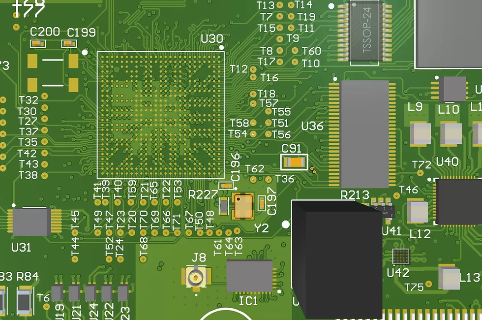
6. Component Placement
Place components within the circuit as per the design and layout guidelines. Occasionally, customers and PCB providers may confer on specific component placement requirements, particularly to avoid electromagnetic interference between specific components.
7. Integrate Drilled Holes
Incorporate drilled holes on the PCB as necessitated by component placement and interconnections. These drilled holes facilitate wire connections across different layers.
8. Routing
Subsequent to component placement and drilled hole insertion, commence the routing process. Routing entails designing pathways connecting circuit components to ensure accurate signal transmission.
9. Incorporate Labels and Identifiers
Add essential labels, identifiers, tags, or reference designators to the layout. These elements serve to indicate the locations and functions of specific components and connections on the PCB.
10. Generate Design/Layout Files
The concluding step involves generating design/layout files for the PCB. These files encompass comprehensive information about the PCB, including component placement, routing, drilling locations, and more. With these files in hand, you are poised for PCB fabrication, assembly, and testing.
This comprehensive guide provides newcomers and electronics enthusiasts with an in-depth understanding of the PCB design process, offering comprehensive guidance. In actual design endeavors, further adjustments and optimizations are often necessary to align with specific project requirements.

Comments